Have questions? Give us a call 920-749-3040
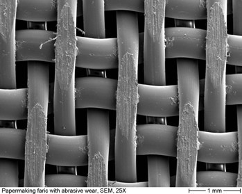
Scanning Electron Microscopy (SEM) is a highly effective and versatile means for investigating textures and structures that are difficult or impossible to see with Light Microscopy. Coatings, surface treatments, fillers, contaminants, surface wear, and interactions between materials are all ideally suited for analysis by SEM. Energy Dispersive X-Ray Spectroscopy (EDS), when operated in tandem with the SEM, enables the analyst to also identify a material’s elemental composition as well as the distribution of the elements within a composite.
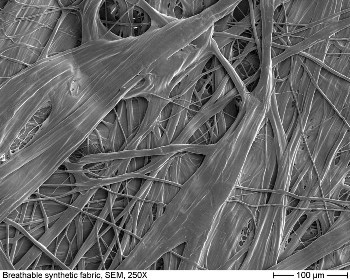
The SEM is not just for extremely small materials. It is also very suitable for viewing objects in the range of a light microscope (10X to 1,000X). The SEM can be superior to the light microscope when viewing transparent or highly porous materials because it has a much greater depth of focus and is not affected by light scatter that can cause loss of detail and contrast.
The SEM capabilities of SGS-IPS Testing are well suited for identifying inorganic contaminants, inclusions, surface defects, and structural characteristics of prepared cross sections. Scanning electron microscopy, either alone or together with Light Microscopy and Infrared Spectroscopy, is ideally suited for solving many of your product or process needs.
SGS-IPS Testing scientists can help you with your microanalysis needs!
Contact our Fiber Science Lab with questions that may require analysis by SEM. 920-749-3040 ext. 1
 |  |